SGM41299C Series Analog Temperature Control Loop Thermal Equilibrium Control
Application Notes2026-07-01
Author: Alcatraz Tong
Corresponding Author: Cherry Cheng
Reviewers: Taylor Tan, Ruoya Yao, Luffy Zhao
ABSTRACT
Modern optoelectronic devices generally require temperature control. Emitter tubes require a constant temperature to ensure wavelength stability, while receiver tubes require low temperatures in high signal-to noise ratio measurement applications to stabilize output impedance and suppress noise. Optoelectronic devices with thermostatic baths, consisting of Peltier-effect TEC (thermoelectric cooling) modules combined with photodiodes and temperature sensors, are very common. Single-chip TEC temperature control devices, such as the SGM41298 and SGM41299C, have emerged as the core components of these thermostatic baths. Taking the SGM41299C as an example, this document explains how to achieve thermal equilibrium in the temperature control loop by detailing the loop’s operating principles and parameter configuration methods.
1 SGM41299C Introduction
The SGM41299C[1] is a monolithic thermoelectric cooling (TEC) thermostat driver device with a two-stage feedback amplifier. The device includes a differential output driver stage, an internal 2.5V output reference voltage, and two zero-drift, rail-to-rail chopper amplifiers. The first chopper amplifier biases the sensed temperature signal and another is an error amplifier for compensating the closed-loop temperature control. This amplifier can be used with a digital controller as well.
The TEC is driven differentially between a linear push-pull stage and a pulse-width modulation (PWM) switching stage. A linear push-pull stage forms one of the arms of the differential output which has a relatively high gain and saturates if the error signal is not close to zero (>2.5%). The means that the TEC is effectively driven by the other arm. The other arm has a low gain, and high-frequency PWM switching driver that can drive the TEC with high efficiency. The PWM switching driver output is passed through an LC filter to remove large voltage ripple before reaching the TEC. It can sink or source current for both the heating and cooling modes connected to the TEC and stabilize its temperature at the set point.
Additionally, the SGM41299C adopts a high efficiency single-inductor architecture with a single-ended to differential driver and low RDSON MOSFETs. It features TEC voltage and current monitoring functions without the need for external sense resistors, and enables independent heating and cooling current/voltage limits programming. The PWM driver operates at a switching frequency of 2.0MHz (typical), is compatible with RTD or NTC thermal sensors, and features a temperature lock indicator. This product has a patent application pending and adopts an environmentally friendly TQFN-6×6-36L green package. It operates over the -40℃ to +125℃ junction temperature range.
2 Basic Principle of Temperature Control Loop
Using the internal components of the SGM41299C, a pure hardware that requires no external interference can be implemented. The structure of the independent temperature control system is shown in Figure 1.
1) The chopper amplifier A1, shown in the red box, is the amplifier circuit for the temperature sensor. In this document, a negative temperature coefficient (NTC) thermistor is used as the temperature sensor. Therefore, A1 is also referred to as the NTC amplifier circuit, with its input being the temperature (mapped to the NTC resistance R) and its output being a voltage. The circuit configuration is shown in Figure 2.
Analyzing the figure above, the output voltage is calculated using equation (1):
Since the NTC is a negative temperature coefficient component, VOUT1 in this circuit is a monotonically increasing function of temperature.
2) The chopping amplifier A2 in the blue box serves as the error amplifier (EA) and the compensation network. Due to the temperature system exhibits hysteresis, lead compensation is required. According to classical control theory, the interaction between the poles and zeros of the compensation network and the inherent poles and zeros of the TEC-NTC (also known as the TEC gain) ensures stable convergence of the loop.
3) The section in the yellow box is the power stage. Its output power varies monotonically with the output of the compensation network, and its voltage gain is limited within the operating range (far lower than the open-loop gain of the compensation amplifier).
4) The section in the green box represents the TEC element. TEC is an active heat exchanger (active heat pump) for electronic transition energy. The direction of heat exchange can be altered by changing the direction of carrier movement (i.e., the polarity of the hot and cold ends can be reversed by changing the bias direction). The basic principle is shown in Figure 3.
Tips: Typically, the TEC’s operating state is controlled so that the cold end temperature varies monotonically with the input power (current), that is, the higher the current, the more heat is transported, the lower the cold end temperature, and the stronger the cooling capacity. During cooling, the TEC’s active heat pump conduction is proportional to the current, while the heat generated by the TEC’s internal resistance is proportional to the square of the current. Continuously increasing the input current may cause the heat generated to exceed the cooling capacity, causing the system to lose its monotonicity. Figure 4 shows the I-V curve of a typical TEC at different thermal power transfer values. As shown in the figure, beyond the peak trace and at higher currents, the monotonicity between the drive voltage and ΔT (the temperature difference between the hot and cold ends) reverses (if the input power were to increase indefinitely, the curve at higher currents in the figure would drop back to zero and even below zero, at which point the entire system’s heating/cooling polarity would reverse). Therefore, the cooling current must be carefully limited below the peak trace to maintain the monotonic relationship between the drive current and the generated ΔT. This is critical for stability and closed-loop convergence.
The simplified signal coupling transmission of the components at the system control level shown in Figure 1 is depicted in Figure 5. The TEC and the temperature-sensing NTC are thermally coupled via the controlled device. Temperature changes (such as heat generated by the optoelectronic device) are external disturbances in the loop.
Taking the temperature rise at NTC as an example, the loop response process is as follows:
The temperature of the controlled device rises → the resistance of the NTC decreases → the output of the NTC amplifier circuit (VOUT1) increases → the absolute value of the error amplifier output increases (manifested as the absolute deviation of VOUT2 from the voltage (VTEMPSET) at the amplifier’s non-inverting input) → the output power increases → the TEC cooling power increases → the temperature of the controlled device decreases. It can thus be seen that this system clearly possesses convergence.
In terms of loop monotonicity, an increase in TEC input power must lead to a decrease in NTC temperature (VOUT1 decreases) to ensure the polarity of the entire negative feedback loop. If an increase in TEC input power is detected while the NTC temperature also rises, this indicates that the thermal system has become unstable. The following sections will discuss how to stabilize the thermal system from the perspectives of thermal coupling mechanisms and loop parameter setting.
3 Heat Transfer System Model
Figure 6 shows a simple structure of a thermostatic bath for optical devices.
According to the law of conservation of energy, system stability requires that the total heating power be less than or equal to the total dissipation power. If this condition is not met, thermal runaway will occur: internal heat accumulation causes the temperature of the TEC’s hot end to rise continuously, resulting in the heat conduction power due to the temperature difference from the hot end to the cold end approaching the active heat pump power from the cold end to the hot end. Consequently, the TEC loses its cooling capability and instead becomes a heat-generating device.
The conditions for ensuring the polarity and monotonicity of the system response include:
1) The heat absorption power of the TEC cold end from the controlled device must exceed the heat leakage power of the outer shell insulation layer;
2) The active heat pump power must be significantly greater than the temperature difference thermal conduction power between the hot and cold ends;
3) The total dissipation capacity must be significantly greater than the system’s total heat generation (the TEC input power plus the heat leakage power of the outer shell). While satisfying the law of conservation of energy, this keeps the TEC hot end at a lower temperature, thereby reducing temperature difference heat transfer.
As shown above, sufficiently low total heat generation, sufficiently high heat sink capacity, and good thermal conduction/coupling are prerequisites for the normal operation of the temperature control loop.
If the system converges in steady state but fails to converge again after introducing a dynamic disturbance (changing the operating state of the controlled device is equivalent to introducing a temperature step error), this indicates that the system’s thermal equilibrium is already at a critical point. The solution is to enhance heat dissipation or reduce the dynamic gain of the compensation network.
4 Circuit Derivation and Parameter Setting
4.1 Temperature Sensing Circuit Derivation
Figure 2 shows the configuration of the temperature sensing amplifier circuit. Based on Equation (1), it can be derived that the gain increases as RFB increases and decreases as R increases. If it is necessary to reduce the gain of the compensation network—that is, to reduce the output gain of the temperature sensing circuit— this can be achieved by decreasing RFB in the temperature sensing amplifier circuit.
4.2 Convergence of Compensation Network
Ignoring details such as thermal coupling and the gain of the amplifier circuit, the components within the orange box are treated as a single unit. Its input is the output VOUT2 of error amplifier A2, and its output is the output VOUT1 of the first temperature measurement amplifier A1. Within its operating range, this system behaves as a monotonic two-port network. The transfer function of the controlled system is denoted as H(s), which represents the TEC gain; the transfer function of the error amplifier and compensation network is denoted as G(s). The entire TEC temperature control system can be simplified as:
When the loop converges, the input to the error amplifier satisfies VOUT1 = VTEMPSET.
4.3 Mathematical Principle of Compensation Network
Generally, once the frequency response or Bode plot of H(s) is known, the poles and zeros of the compensation transfer function G(s) can be designed appropriately. However, temperature control systems are unique due to their significant time delay.
Figure 9 shows the TEC gain Bode plot for a typical thermostatic bath optical device (which also reflects the characteristic roots of the transfer function H(s)). Two poles are present within the visible bandwidth, one in the mHz range and the other in the Hz range, which are difficult for general-purpose equipment to measure accurately. Such a two-pole system presents a major issue: when the system gain is increased, both poles inevitably fall within the bandwidth, causing the gain to decay at a rate of -40dB/decade at very low frequencies. This leads to system instability, a low crossover frequency, and slow response times.
The compensation function G(s) requires two corresponding zeros to offset the effects of these two poles. Additionally, a low-frequency pole is introduced as the main pole to increase low-frequency gain (thereby reducing steady-state error), and another pole is introduced between the crossover frequency and ten times the crossover frequency to control phase and gain margins. The objective is to obtain a suitable compensated transfer function H(s)*G(s) with sufficiently high low-frequency gain, a single effective pole before the crossover frequency, and a phase margin controlled between 45° and 60°.
4.4 Zero-Pole Distribution of Compensation Network
Based on the above analysis, the compensation transfer function must have one low-frequency pole, two zeros to compensate for in-band poles, and at least one out-of-band pole near the crossover frequency (fcross) to ensure sufficient phase and gain margins. Type III[3] compensation circuit can provide up to two zeros and three poles, making them a suitable choice.
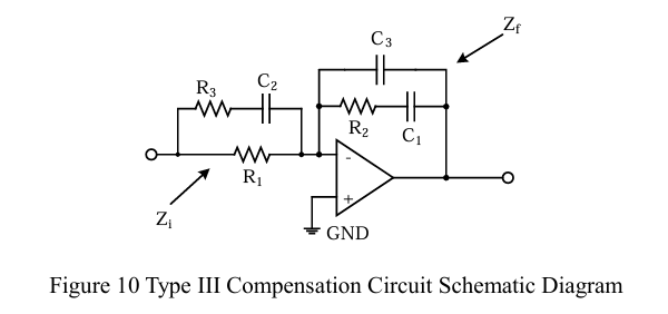
By analyzing Figure 10, the formula for the transfer function H(s) can be obtained as follows (typically, C1 ≫ C3 is assumed for approximate calculations):
The corresponding zeros and poles are as follows:
The distribution of zeroes and poles across the bandwidth (including the actual graph and the zero-pole line graph) is shown in Figure 11.
Typically, fp1 is taken as the first pole outside the GBW, while the role of fp2 can be disregarded for now. The parameters to be calculated include:
- fp0: the main pole (the only effective pole within the band);
- fz1, fz2: used to eliminate two poles within the TEC gain bandwidth;
- fp1: located between the crossover frequency and 10 times the bandwidth, used to control phase margin.
4.5 PID Parameter Tuning Method
As mentioned earlier, it is difficult to accurately measure the in-band poles of the TEC gain, and compensation network parameters derived solely from guesswork are not optimal. In practice, tuning is often performed using the PID critical parameter method.
Under certain conditions, Type III compensation circuit can be simplified into proportional, integral, and derivative equations, with the corresponding components labeled P (Proportional), I (Integral), and D (Derivative). In the figure below, it is still assumed that CI >> CF.
For the two chopper amplifiers inside the SGM41299C, the following tuning steps are recommended:
1) Single-ratio Control
When CD is open-circuited and CI is short-circuited, the circuit operates in single-ratio control mode. First, select an RI value (100kΩ or higher is recommended to allow for subsequent adjustments), then gradually increase the RP/RI ratio until slight oscillation is observed at OUT2; this indicates the critical ratio parameter. Divide this ratio by 2 to obtain the actual usable ratio value; typically, RP/RI < 1.
2) Adding Integral Term
Connect the integrating capacitor CI to the system and gradually decrease CI (the integral term is amplified, since the RC integration output is inversely proportional to R*C) until critical oscillation occurs at OUT2. Divide the capacitance value of CI at this critical state by 2 to obtain the usable integral term parameter.
3) Adding Derivative term
Short-circuit RD and connect a capacitor CD with a value much smaller than CI. Gradually increase the capacitance of CD until oscillation occurs at OUT2 (critical point). At this point, the circuit can be stabilized again by reducing the capacitance of CD or by reconnecting RD. The gain of the derivative term is inversely proportional to the values of RD and CD.
4) Feedback Capacitor
Introducing a feedback capacitor CF in the pF to nF range can further enhance the stability of the loop.
5 Conclusion
In summary, to maintain thermal equilibrium in an analog temperature control system, it is first necessary to ensure that the system can converge under steady-state conditions. Once heat dissipation has been improved, adjustments can be attempted by reducing the gain of the compensation network, without the need to recalculate all parameters.
Methods for reducing the gain of the compensation network include:
1) Reducing the RFB of the temperature sensing amplifier circuit;
2) Reducing the RP/RI ratio;
3) Increasing RD or reducing CD.
In practical applications, in addition to theoretical calculations and PID tuning, attention must also be paid to practical issues such as thermal design of the PCB layout, selection and placement of NTC, and matching of TEC driving capability. A well-designed thermal structure and reasonable loop parameters jointly determine the system’s temperature control accuracy, stability, and response speed.
6 References
[1] SG Micro Corp. SGM41299C Datasheet[EB/OL]. https://www.sg-micro.com/rect/assets/47c8d32e-586a-46ce-b5a5-5a688fa8f41b/SGM41299C.pdf
[2] Mayursinh D. Thakor, S. K. Hadia, Ashok Kumar. Precise Temperature Control through Thermoelectric Cooler with PID Controller[C]. April 2015.
[3] Texas Instruments Incorporated. Demystifying Type II and Type III Compensators Using Op-Amp and OTA for DC/DC Converters[EB].
Products
Related files

ANE202606001 REV.A.pdf
